A Complete Guide to Wafer Inspection, Defect Detection, Quality Control, and Failure Analysis
Modern semiconductor manufacturing depends on extreme precision. As chip designs become smaller and more complex, manufacturers must identify microscopic defects before they affect device performance, reliability, or production yield. This is where a semiconductor microscope becomes indispensable.
A semiconductor inspection microscope is used throughout the production process to support wafer inspection, defect detection, quality control, and failure analysis. From detecting contamination on silicon wafers to evaluating advanced packaging structures, microscopy enables engineers to identify issues early, improve manufacturing efficiency, and maintain product quality.
In today’s competitive semiconductor industry, inspection technologies are no longer limited to simple visual checks. Advanced imaging systems, digital microscopes, AI-assisted analysis tools, and automated inspection platforms are transforming how manufacturers approach yield improvement, process monitoring, and root cause investigation.
Why Semiconductor Inspection Matters More Than Ever
The semiconductor industry is experiencing rapid growth driven by artificial intelligence, high-performance computing, automotive electronics, data centers, and advanced consumer devices. At the same time, chip geometries continue shrinking, making defects increasingly difficult to detect.
A particle only a few microns in size can cause electrical failures, reduce manufacturing yield, or compromise long-term reliability. As a result, manufacturers rely heavily on advanced inspection systems to identify problems before they become costly failures.
Key objectives of semiconductor inspection include:
- Improving manufacturing yield
- Reducing defect-related losses
- Ensuring product reliability
- Monitoring process consistency
- Supporting regulatory and quality requirements
- Accelerating root cause analysis
Microscopy plays a critical role in achieving these goals.
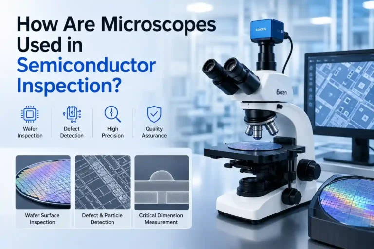
What Is a Semiconductor Inspection Microscope?
Manufacturers often choose different microscope systems depending on their inspection requirements. For example, digital microscopes, stereo microscopes, and metallurgical microscopes are commonly used for semiconductor wafer inspection and packaging analysis.
A semiconductor inspection microscope is a specialized imaging system designed to examine wafers, dies, integrated circuits, and packaging structures at high magnifications.
Unlike conventional laboratory microscopes, semiconductor inspection systems often include advanced lighting, measurement software, image processing tools, and automation capabilities.
These microscopes help engineers perform:
- Wafer defect inspection
- Surface analysis
- Contamination detection
- Pattern verification
- Packaging inspection
- Failure diagnostics
- Dimensional measurement
Different microscope technologies are used depending on the inspection task.
Optical Microscopes
Optical microscopes remain one of the most widely used tools in semiconductor manufacturing.
Advantages include:
- Fast inspection speed
- Large viewing area
- Non-destructive analysis
- Cost-effective operation
They are commonly used for routine wafer inspection and production-line quality checks.
Digital Microscopes
Digital microscopes combine optical imaging with high-resolution cameras and analysis software.
Benefits include:
- Image capture and documentation
- Real-time measurement
- Automated reporting
- Enhanced image processing
Digital systems are particularly useful for quality control and defect documentation.
Stereo Microscopes
Stereo microscopes provide a three-dimensional view of components and packaging structures.
Applications include:
- Wire bond inspection
- Solder joint evaluation
- Package assembly verification
- Component alignment checks
The depth perception offered by stereo systems makes them valuable for packaging inspections.
Failure Analysis Microscopes
A failure analysis microscope is used when engineers need to determine why a semiconductor device failed.
These systems may include:
- High-resolution optical imaging
- Polarized illumination
- Digital analysis tools
- Advanced measurement functions
Failure analysis microscopes help locate defects and identify root causes quickly.
Wafer Inspection: The Foundation of Semiconductor Quality
One of the most important applications of a wafer inspection microscope is examining silicon wafers during fabrication.
A single defect introduced early in the manufacturing process can affect thousands of devices on a wafer. Detecting these issues before additional processing occurs saves time and reduces production costs.
Surface Defect Inspection
Engineers inspect wafers for:
- Scratches
- Surface pits
- Residue
- Stains
- Mechanical damage
High-resolution imaging enables early identification of defects that may affect device functionality.
For high-resolution wafer surface evaluation, many manufacturers utilize specialized digital imaging systems capable of detecting contamination, scratches, and process-related defects.
Pattern Defect Detection
Photolithography processes create intricate circuit patterns on semiconductor wafers.
Microscopes help detect:
- Missing features
- Pattern collapse
- Bridging defects
- Line-width variations
- Misaligned structures
Accurate pattern inspection is essential for advanced semiconductor nodes.
Contamination Detection
Particles and contaminants are among the leading causes of yield loss.
A wafer inspection microscope helps engineers identify:
- Dust particles
- Process residues
- Organic contamination
- Foreign materials
Early contamination detection reduces manufacturing defects and improves production consistency.
Alignment and Overlay Inspection
Multiple layers must be aligned precisely during semiconductor fabrication.
Microscopy allows engineers to verify:
- Overlay accuracy
- Layer positioning
- Registration quality
Even minor alignment errors can impact electrical performance.
How Microscopes Support Semiconductor Defect Detection
Semiconductor defect detection is one of the most critical functions of inspection microscopy.
Defects can originate from materials, equipment, process variation, handling, or packaging operations.
Scratch Detection
Mechanical scratches can occur during:
- Wafer transport
- Cleaning procedures
- Manufacturing processes
Microscopes reveal damage that may be invisible to the naked eye.
Particle Analysis
Particle contamination remains a major challenge in semiconductor manufacturing.
Inspection systems help determine:
- Particle size
- Distribution patterns
- Potential contamination sources
This information supports process optimization and contamination control programs.
Crack Identification
Microscopic cracks can develop due to:
- Thermal stress
- Mechanical handling
- Dicing operations
- Packaging processes
Early crack detection helps prevent field failures and warranty claims.
Bonding Defect Inspection
Bonding defects can compromise electrical performance and package reliability.
Microscopes are used to inspect:
- Wire bonds
- Flip-chip connections
- Micro-bumps
- Interconnect structures
Accurate imaging supports both production quality and reliability testing.
Microscopes in Semiconductor Quality Control
Effective semiconductor quality control requires inspection throughout the manufacturing process.
Microscopes provide the visual data needed to verify compliance with design specifications and process standards.
Incoming Material Inspection
Before production begins, raw materials and wafers are evaluated for defects.
Inspection focuses on:
- Surface quality
- Contamination levels
- Material consistency
In-Process Inspection
Production-stage inspections help identify problems before they spread through the manufacturing line.
Engineers use microscopes for:
- Process monitoring
- Defect tracking
- Equipment validation
- Yield management
Final Product Verification
Completed devices undergo inspection before shipment.
Typical evaluation criteria include:
- Package integrity
- Bond quality
- Surface appearance
- Marking verification
Microscopy ensures products meet customer and industry requirements.
Failure Analysis at Wafer and Packaging Levels
When semiconductor devices fail, engineers must determine exactly why.
This process is known as semiconductor failure analysis.
A failure analysis microscope helps investigators identify the origin of defects and understand the mechanisms behind device failure.
Root Cause Analysis
Failure analysis begins by locating the defective area.
Potential causes include:
- Process variation
- Material defects
- Electrical overstress
- Mechanical damage
- Contamination
Identifying the root cause enables corrective actions that improve future production.
Cross-Section Evaluation
Cross-sectional analysis allows engineers to examine internal structures.
This technique reveals:
- Layer integrity
- Voids
- Delamination
- Structural defects
Cross-sectional imaging is especially important in advanced semiconductor technologies.
Advanced Packaging Inspection
Modern semiconductor devices increasingly rely on advanced packaging architectures.
Examples include:
- Chiplets
- 2.5D integration
- 3D packaging
- Through-silicon vias (TSVs)
These structures require detailed semiconductor packaging inspection to verify assembly quality and reliability.
Wire Bond and Solder Joint Inspection
Packaging defects often occur at electrical connection points.
Microscopes help evaluate:
- Bond strength
- Joint integrity
- Alignment accuracy
- Surface condition
Proper inspection reduces reliability risks and field failures.
AI-Powered Inspection Is Transforming Semiconductor Manufacturing
Artificial intelligence is becoming an increasingly important part of semiconductor inspection workflows.
Traditional inspection methods rely heavily on human operators. AI-based systems can analyze images faster and identify subtle defect patterns that may be difficult to detect manually.
Automated Defect Classification
AI systems can automatically classify:
- Scratches
- Contamination
- Cracks
- Pattern defects
- Packaging abnormalities
This reduces inspection time and improves consistency.
Smart Image Analysis
AI-powered image processing enhances:
- Defect recognition
- Feature extraction
- Measurement accuracy
- Reporting efficiency
Yield Improvement Through Data Analytics
Inspection data can be linked with manufacturing processes to identify trends and recurring issues.
Benefits include:
- Faster process optimization
- Reduced defect rates
- Improved production yield
- Better predictive maintenance
As semiconductor manufacturing continues evolving, AI-assisted microscopy will play an increasingly important role in quality assurance and process control.
How to Choose the Right Semiconductor Inspection Microscope
Selecting the appropriate microscope depends on the application and inspection requirements.
Consider the following factors:
Magnification Range
Different inspections require different magnification levels.
Routine inspections may only need moderate magnification, while detailed failure analysis often requires much higher imaging capability.
Image Resolution
Higher resolution allows engineers to identify smaller defects and improve measurement accuracy.
Lighting Options
Semiconductor surfaces can be highly reflective.
Advanced illumination techniques improve contrast and reveal subtle defects.
Measurement Functions
Modern digital microscopes often include:
- Dimensional measurement
- Defect annotation
- Automated reporting
- Data management
Automation Capability
Automated inspection systems can significantly improve throughput and consistency in high-volume manufacturing environments.
Frequently Asked Questions (FAQ)
A semiconductor microscope is used for wafer inspection, defect detection, quality control, packaging inspection, and failure analysis throughout the semiconductor manufacturing process.
A wafer inspection microscope with high-resolution optics, digital imaging, and advanced illumination is typically preferred for routine wafer analysis and defect identification.
Even microscopic defects can reduce yield, cause electrical failures, and affect product reliability. Early defect detection helps manufacturers prevent costly production losses.
Wafer inspection focuses on identifying defects during production, while failure analysis investigates the root causes of defects after a failure has occurred.
Yes. AI-assisted inspection systems can automate defect classification, improve accuracy, reduce manual workload, and accelerate yield improvement efforts.
Microscopy enables engineers to verify process consistency, identify defects, inspect packaging structures, and ensure products meet required quality standards.
Conclusion
As semiconductor devices become more advanced, the need for accurate inspection continues to grow. A modern semiconductor inspection microscope serves as a critical tool for wafer inspection, semiconductor defect detection, quality control, and failure analysis.
From identifying contamination on silicon wafers to evaluating advanced packaging structures, microscopy provides the detailed visual information needed to improve yield, enhance reliability, and support continuous process improvement.
Manufacturers that invest in high-performance semiconductor microscopes, digital imaging systems, and AI-powered inspection technologies will be better equipped to meet the demands of next-generation semiconductor production while maintaining the highest standards of quality and performance.
Recommended Microscope Solutions for Semiconductor Inspection
Selecting the right microscope depends on your inspection workflow, magnification requirements, and imaging needs. Murzider provides professional microscope solutions for semiconductor wafer inspection, defect analysis, quality control, and advanced packaging inspection.