Quick Answer
For most soldering, PCB inspection, and electronics manufacturing tasks, a solder joint inspection microscope with 5X–50X magnification, long working distance, and bright LED illumination provides the best balance of image quality, comfort, and efficiency. A stereo microscope is typically preferred because it offers true 3D depth perception, making it easier to inspect solder joints, identify defects, and perform rework. For documentation and measurement tasks, a digital microscope may be the better choice.
Why Solder Joint Inspection Matters
Modern electronic devices rely on thousands of solder joints to create reliable electrical and mechanical connections. Even a small defect can lead to product failures, intermittent connections, overheating, or reduced lifespan.
Common solder joint defects include:
- Cold solder joints
- Solder bridges
- Insufficient solder
- Excess solder
- Voids and porosity
- Cracked solder joints
- Poor wetting
- Component misalignment
A professional solder joint inspection microscope helps manufacturers, quality control teams, and repair technicians detect these defects before products reach customers.

What Is a Solder Joint Inspection Microscope?
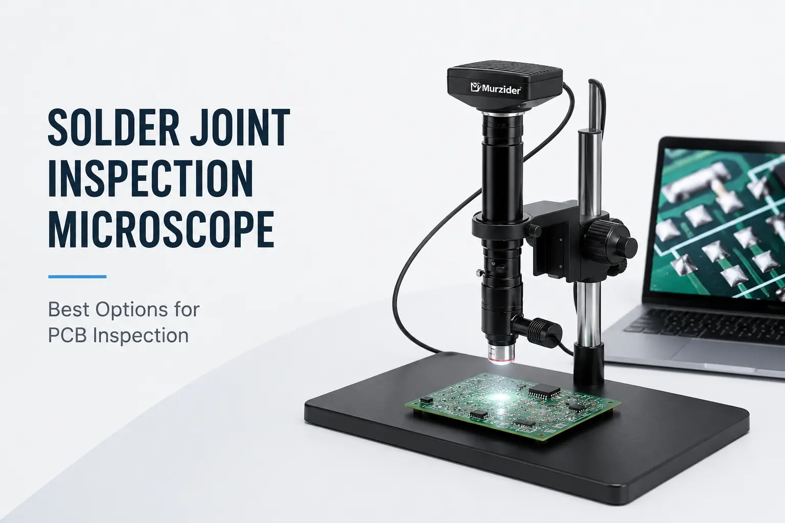
A solder joint inspection microscope is a specialized microscope used to examine solder connections on printed circuit boards (PCBs), electronic assemblies, SMT components, and other precision electronic devices.
Unlike standard laboratory microscopes, inspection microscopes provide:
- Lower magnification ranges optimized for electronics
- Long working distances
- Large fields of view
- Enhanced lighting systems
- Comfortable viewing for extended use
These features make them ideal for electronics manufacturing and quality control applications.
Key Features to Look for in a Solder Joint Inspection Microscope
Magnification Range
One of the most common mistakes is assuming higher magnification always produces better inspection results. Understanding the relationship between magnification and resolution is essential when selecting a microscope for electronics inspection.
For most applications:
| Application | Recommended Magnification |
|---|---|
| General PCB inspection | 5X–20X |
| Solder joint inspection | 10X–40X |
| SMT component inspection | 20X–50X |
| Failure analysis | 50X–100X |
For routine electronics inspection, a solder joint inspection microscope with 10X–40X magnification is usually sufficient.
Working Distance
Working distance refers to the space between the objective lens and the workpiece.
A longer working distance allows operators to:
- Move tools freely
- Perform soldering repairs
- Rework components
- Handle larger PCB assemblies
For electronics applications, a working distance of at least 100 mm is generally recommended.
Depth Perception
Depth perception is critical when inspecting solder joints.
A stereo microscope provides:
- True three-dimensional viewing
- Better defect recognition
- Improved hand-eye coordination
- Easier soldering and rework
This is why many professionals prefer stereo microscopes over digital-only systems.
Lighting Quality
Proper illumination significantly improves inspection accuracy.
Recommended lighting options include:
LED Ring Lights
Ideal for general PCB and solder inspection.
Adjustable LED Lighting
Allows users to optimize contrast and eliminate shadows.
Polarized Lighting
Helpful when inspecting reflective solder surfaces and metallic components.
Good lighting often improves inspection quality more than increasing magnification.
Stereo Microscope vs Digital Microscope for Solder Joint Inspection
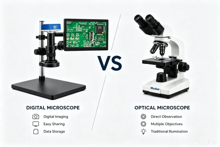
Choosing between a stereo microscope and a digital microscope depends on the application. If you’re comparing imaging technologies, see our guide on digital microscope vs optical microscope.
| Feature | Stereo Microscope | Digital Microscope |
|---|---|---|
| 3D Viewing | Excellent | Limited |
| Eye Comfort | Excellent | Excellent |
| Soldering Rework | Excellent | Good |
| Documentation | Limited | Excellent |
| Measurements | Basic | Advanced |
| Image Capture | Optional | Built-in |
| Training & Sharing | Limited | Excellent |
For most soldering, PCB inspection, and rework applications, stereo microscopes remain the preferred choice because they provide true depth perception and comfortable long-term viewing.
For quality documentation and reporting, a digital microscope offers additional advantages.
Best Microscope Configurations for Solder Joint Inspection
Entry-Level Electronics Inspection
Suitable for:
- Hobbyists
- Repair technicians
- Small workshops
Recommended Features:
- Stereo microscope
- 10X–40X zoom
- LED ring light
- Boom stand
Professional PCB Inspection
Suitable for:
- Electronics manufacturers
- SMT assembly lines
- Quality control departments
Recommended Features:
- Trinocular stereo microscope
- 7X–45X zoom range
- Camera system
- Adjustable LED lighting
This setup provides excellent flexibility for both inspection and documentation.
For image capture, documentation, and measurement tasks, industrial digital microscopes can provide additional workflow advantages.
Advanced Quality Control Inspection
Suitable for:
- High-volume production facilities
- Semiconductor packaging
- Failure analysis laboratories
Recommended Features:
- High-resolution digital camera
- Measurement software
- Motorized inspection system
- Advanced lighting options
Common Applications of a Solder Joint Inspection Microscope
PCB Inspection
Inspect solder joints, traces, vias, and component placement on printed circuit boards. Learn more about choosing the right PCB inspection microscope for electronics manufacturing and quality control.
SMT Inspection
Verify proper placement and solder quality of surface-mount components.
Electronics Repair
Identify damaged components, poor solder connections, and manufacturing defects.
Connector Inspection
Examine terminals, contacts, and soldered connections in electrical connectors.
EV Electronics Manufacturing
Inspect high-reliability solder joints used in battery management systems, power modules, and vehicle control units.
Common Solder Joint Defects Visible Under a Microscope
A quality solder joint inspection microscope can help identify:
Cold Solder Joints
Appear dull, rough, or grainy and often cause unreliable electrical connections.
Solder Bridges
Unwanted solder connections between adjacent pads or leads.
Insufficient Solder
Incomplete coverage resulting in weak mechanical strength.
Cracked Joints
Often caused by vibration, thermal cycling, or mechanical stress.
Voids
Internal cavities that reduce conductivity and long-term reliability.
Early detection helps reduce manufacturing costs and product failures.
How to Choose the Right Solder Joint Inspection Microscope
When selecting a solder joint inspection microscope, consider:
- Magnification requirements
- Working distance
- Lighting quality
- Camera integration
- Documentation needs
- Available workspace
- Future inspection requirements
Most manufacturers find that a stereo microscope with 7X–45X zoom and LED ring illumination provides the best overall value.
If you’re evaluating different microscope configurations for electronics inspection, PCB assembly, or manufacturing quality control, our comprehensive microscope selection guide can help you compare options and choose the right system.
Conclusion
Choosing the best solder joint inspection microscope depends on your inspection requirements, production environment, and documentation needs. For most PCB assembly, SMT manufacturing, and electronics repair applications, a stereo microscope with 5X–50X magnification, long working distance, and LED ring illumination provides the ideal balance of performance and usability.
Whether you are inspecting solder joints on prototype boards or performing quality control in high-volume production, the right microscope can significantly improve inspection accuracy, reduce defects, and increase manufacturing efficiency.
Frequently Asked Questions
For most PCB quality control and SMT (Surface Mount Technology) applications, a magnification range of 10X–40X is ideal. Professional systems, like the Murzider stereo zoom series, deliver sufficient optical resolution to detect micro-defects (such as cold solder joints and solder bridging) within this range without sacrificing the field of view (FOV) or reducing operator efficiency.
Yes, for manual soldering and PCB rework, a stereo microscope is superior. A stereo optical system provides true 3D depth perception and real-time, lag-free viewing, which are critical for precise hand-eye coordination. However, Murzider’s digital inspection microscopes are excellent alternatives if your workflow prioritizes component documentation, automated measurements, and team viewing on a monitor.
Not strictly required for physical inspection, but highly recommended for quality assurance (QA). Integrating a high-definition Murzider microscope camera allows for digital image capture, defect logging, training, and generating standard-compliant inspection reports for customer communication and compliance.
Adjustable LED ring lights are the industry standard because they provide bright, uniform, and shadow-free illumination. For highly reflective solder fillets and metallic components, Murzider recommends using a polarizing filter or coaxial illumination to eliminate harsh glare and hotspots that can hide micro-cracks.
Yes. Many Murzider trinocular stereo microscopes and long working distance (LWD) digital systems are engineered specifically for both tasks. They offer the necessary clearance (typically 100mm+) for soldering iron access during PCB rework while providing the optical clarity needed for rigorous quality control inspection.