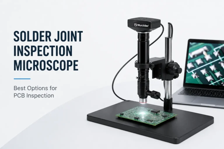
Quick Answer
For most PCB inspection applications, a stereo microscope with 10X–80X magnification is the best choice. It provides excellent depth perception, sufficient working distance for soldering and rework, and clear visualization of PCB components and solder joints. For documentation, measurement, and quality reporting, a digital microscope with an integrated camera system may be the preferred solution.
Printed Circuit Boards (PCBs) are at the heart of modern electronics. As electronic components become smaller and circuit designs more complex, choosing the right microscope for PCB inspection is more important than ever. Defects such as solder bridges, misaligned components, damaged traces, and contamination can significantly impact product quality and reliability.
Selecting the right microscope helps manufacturers improve inspection accuracy, increase productivity, and reduce costly defects.
Quick Answer
For most PCB inspection applications, a stereo microscope with 10X–80X magnification is the best choice.
It provides excellent depth perception, sufficient working distance for soldering and rework, and clear visualization of PCB components and solder joints. When image capture, measurement, defect documentation, and quality reporting are required, a digital microscope with an integrated camera system is often the preferred solution.
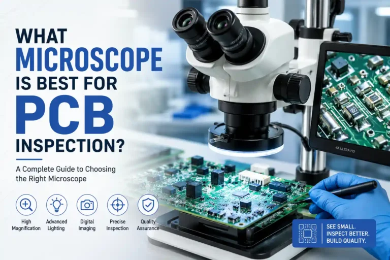
Why PCB Inspection Requires the Right Microscope
Printed Circuit Boards (PCBs) are at the heart of modern electronics. As components become smaller and circuit layouts more complex, selecting the right microscope for PCB inspection is increasingly important.
Common defects—including solder bridges, misaligned components, damaged traces, and contamination—can significantly affect product quality and reliability. The right microscope helps manufacturers improve inspection accuracy, increase productivity, and reduce costly defects.
For many electronics manufacturing and repair applications, stereo microscopes offer the best balance of magnification, working distance, and depth perception.
Why PCB Visual Inspection Is Important?
Effective PCB visual inspection helps manufacturers identify solder defects, damaged traces, contamination, and component placement issues before products reach customers.
Five Key Factors to Consider
1. Choose the Right Microscope Type
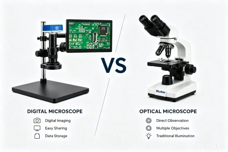
For most PCB inspection applications, a stereo microscope for PCB inspection and a digital microscope are the two primary options available to manufacturers.
A PCB inspection digital microscope provides large-screen viewing, image capture, measurement tools, and remote collaboration capabilities that are increasingly important in modern electronics production.
Stereo microscopes provide true three-dimensional viewing and natural depth perception, making them ideal for soldering, rework, and manual inspection. Digital microscopes offer image capture, measurement tools, and large-screen viewing for documentation and collaboration.
For many electronics manufacturers, a trinocular stereo microscope offers the best combination of optical inspection and digital imaging capabilities.
Related Reading: Microscope Selection Guide: How to Choose the Right Microscope for Your Application
2. Optical Quality Matters
High-quality optics ensure sharp images, accurate color reproduction, and reliable defect identification. Poor optical performance can make small defects difficult to detect and reduce inspection efficiency.
3. Ergonomics Improve Productivity
PCB inspection often requires long working hours. Adjustable viewing angles, comfortable eyepieces, and ergonomic designs help reduce operator fatigue and improve consistency.
4. Portability and Flexibility
Boom stands and articulating arm systems allow inspectors to position the microscope precisely where needed. Flexible configurations are especially valuable for larger PCB assemblies.
5. Upgrade Potential
As inspection requirements evolve, the ability to add cameras, displays, and measurement software can extend the lifespan of your microscope investment.
Essential Features of a PCB Inspection Microscope
Magnification Range
Most PCB inspection tasks can be completed within a 10X to 80X magnification range.Related Reading: What Is the Difference Between Magnification and Resolution? Higher magnification may be required for microelectronics analysis and failure investigation.
Working Distance
A long working distance provides sufficient space for soldering irons, tweezers, and rework tools. This is particularly important for repair and assembly tasks.
Depth of Field
Good depth of field allows inspectors to view components at different heights without constant refocusing, improving efficiency and accuracy.
Lighting
Proper illumination is critical. Adjustable LED ring lights provide even lighting, while polarized lighting can reduce reflections from shiny PCB surfaces.
Image Quality
Resolution, color accuracy, and optical clarity all contribute to effective defect detection and analysis.
| Inspection Task | Recommended Magnification |
|---|---|
| General PCB Inspection | 10X–40X |
| SMT Component Inspection | 20X–80X |
| Fine-Pitch Solder Joints | 40X–100X |
| Failure Analysis | 100X–200X |
| Microelectronics Inspection | 200X+ |
The Role of Digital Imaging Systems
A high-quality PCB inspection microscope camera can significantly improve defect detection, documentation, and process traceability in electronics manufacturing.
Digital imaging systems have become increasingly important in electronics manufacturing.
Benefits include:
- Real-time observation
- Defect documentation
- Process traceability
- Quality reporting
- Team collaboration
For image capture, 5MP cameras are suitable for basic documentation, while 10MP and 20MP systems provide higher detail for advanced inspection. 4K camera systems deliver exceptional image quality and large-screen viewing capabilities.
Common Selection Mistakes
When purchasing a PCB inspection microscope, avoid these common mistakes:
- Choosing more magnification than necessary
- Ignoring working distance requirements
- Underestimating lighting quality
- Focusing only on camera resolution
- Overlooking ergonomics
How Much Does a PCB Inspection Microscope Cost?
The PCB inspection microscope price varies depending on magnification range, optical quality, camera resolution, and stand configuration. Entry-level systems may be suitable for educational use, while advanced industrial solutions with 4K imaging and measurement software are designed for professional electronics manufacturing.
There is no single microscope that fits every PCB inspection application. Stereo microscopes excel in repair and rework, while digital microscopes offer superior documentation and collaboration features.
For many electronics manufacturers, a trinocular stereo microscope combined with a high-resolution camera system provides the ideal balance of inspection performance, flexibility, and long-term value.
If you are unsure which microscope best suits your application, Murzider can help you identify the right PCB inspection solution based on your workflow, budget, and inspection requirements.
Expert Tip from Murzider
For PCB inspection, magnification alone should not determine your purchasing decision. Optical quality, working distance, lighting, and imaging capabilities often have a greater impact on inspection efficiency and defect detection accuracy.
Frequently Asked Questions
For most PCB inspection tasks, a stereo microscope is the preferred choice because it provides 3D viewing, good depth perception, and sufficient working distance for inspection, soldering, and rework.
Most PCB inspection applications require 10X–80X magnification. Fine-pitch solder joints and microelectronics inspection may require magnifications above 100X.
Yes. Digital microscopes are ideal for image capture, measurement, defect documentation, quality reporting, and remote collaboration in electronics manufacturing.
A longer working distance provides space for soldering irons, tweezers, probes, and rework tools, making inspection and repair tasks easier and safer.
Key features include optical quality, appropriate magnification, long working distance, good depth of field, adjustable LED lighting, and optional camera integration for documentation.